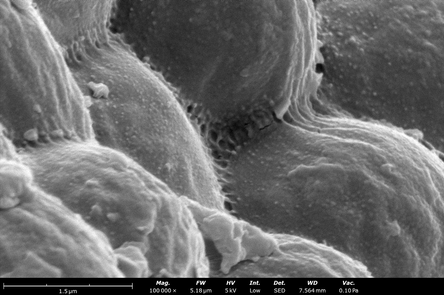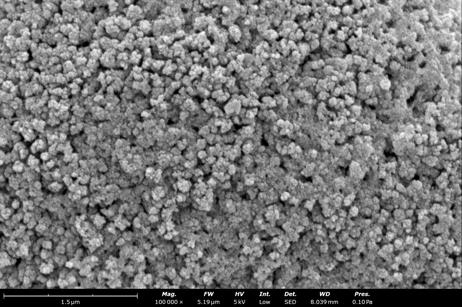
High Resolution Imaging
Visualize your materials' surface morphology and topography at the nanoscale with exceptional clarity and precision and identify critical defects, interfaces, or features of interest.
Elemental Analysis (EDS)
Point, line scan and area mapping are available. EDS maps can be acquired up to 960×960 pixels and line scans of 512 pixels. The elemental detection capability is from Boron to Americium.
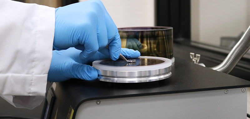
Sample Prep
Methods include: non-destructive sample mounting, non-conductive sample coatings, mechanical cutting/polishing, cross sectional polishing, and powder deposition.
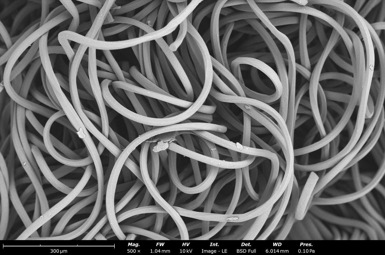
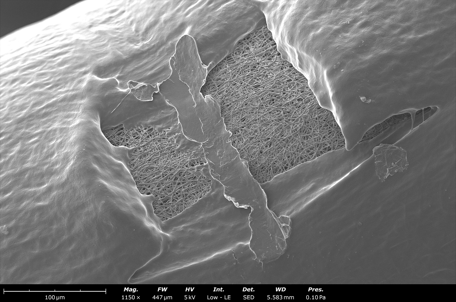
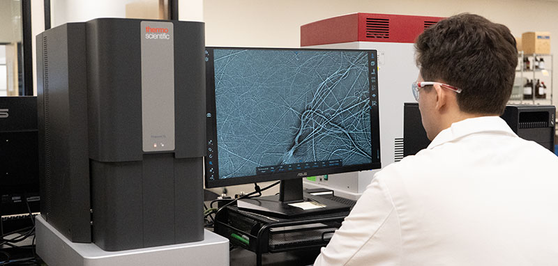
Fiber Analysis
Automated fiber analysis via SEM imaging produces accurate size and orientation information of micro and nanofibers, including complex fiber networks.
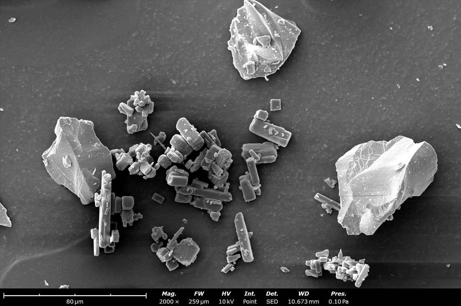
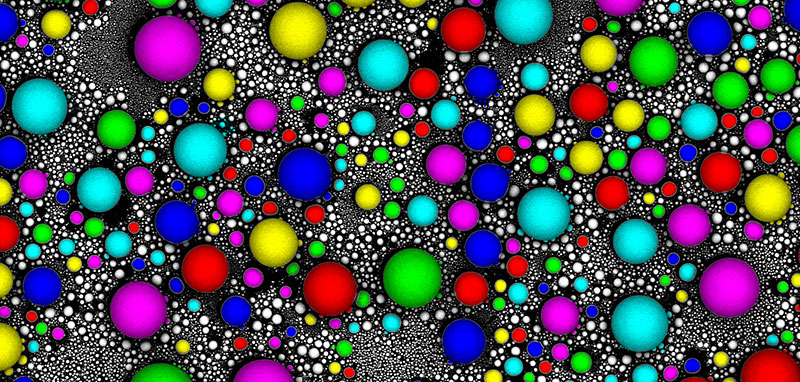
Particle Analysis
Automated, high-speed analysis to gather statistically relevant and accurate data on particle size and morphology of submicron particles. Pair with EDS for particle-by-particle compositional analysis.
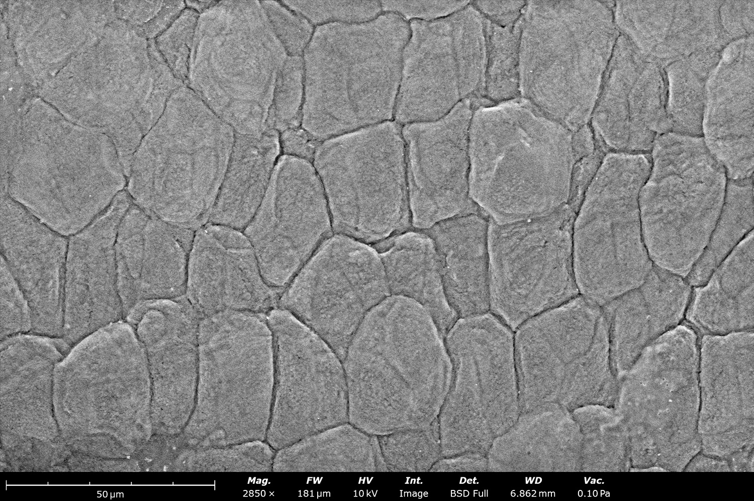
Pore Analysis
Automated pore analysis measurements provide a better understanding of the characteristics of porous materials by providing pore sizes, aspect ratios, and distribution of pores.